

William Parker
I research hybrid bonding and wafer-level bonding technologies used in advanced semiconductor integration. My work focuses on direct bonding, interconnect density, alignment requirements, process control, yield, and the potential role of hybrid bonding in next-generation memory and logic systems. I publish on this website because hybrid bonding represents an important shift in how semiconductor components can be interconnected. As conventional interconnect scaling becomes more challenging, direct bonding approaches may provide new ways to achieve extremely dense electrical connections. My research follows hybrid bonding applications in advanced memory, 3D integration, image sensors, logic, and heterogeneous packaging. I examine process requirements, equipment needs, materials, bonding accuracy, and manufacturing yield. I also track the equipment and materials ecosystem supporting hybrid bonding. The transition from research demonstrations to high-volume manufacturing requires reliable processes and production infrastructure. Through my articles, I aim to explain the technology behind hybrid bonding and evaluate how bonding density, process maturity, manufacturing capacity, and cost influence its adoption.
Hybrid bonding analyst covering wafer bonding, direct interconnects, 3D integration, alignment, process control, equipment, materials, and manufacturing yield.
William Parker is an advanced packaging researcher specializing in hybrid bonding and wafer-level bonding technologies. His work examines direct interconnects, bonding accuracy, process control, yield, and high-density semiconductor integration.
William follows hybrid bonding applications across advanced memory, logic, image sensors, 3D integration, and heterogeneous packaging. He studies how direct bonding can enable higher interconnect density and shorter electrical connections.
Manufacturing maturity is a major part of his research. Bonding accuracy, surface preparation, process stability, yield, equipment capability, and material requirements all influence whether hybrid bonding can move into high-volume production.
William also tracks the equipment and materials ecosystem supporting the technology. Through his articles, he explains the technical and manufacturing factors that may determine the pace of hybrid bonding adoption.
His Articles

Options Protection for Semi ETFs – Empirical Cost-Benefit of Put Option Hedging
Semiconductor themed ETFs can deliver spectacular upside when the cycle is friendly, but they also carry a very real downside: sharp, sudden drawdowns when sentiment turns, earnings disappoint, or macro conditions tighten. Options, particularly put options, are one of the most direct ways to protect against those swings. The challenge is not whether puts work; they clearly do. The challenge is how to fit the cost of protection to the reality of the ETF’s behavior so you do not overpay for insurance or hedge at the wrong strikes and tenors.

ASICs Eating into GPU Share: Broadcom and Marvell’s Golden Era
For much of the last decade, GPUs have been the default answer to almost any question about high‑performance compute and AI acceleration. They offered flexible parallelism, strong software ecosystems, and a simple story: one architecture, many workloads. That narrative is starting to fragment. In more data‑center racks and custom systems, application‑specific integrated circuits (ASICs) are quietly claiming sockets that might once have gone to GPUs.
HBM’s Crowding-Out Effect on DRAM Capacity: Supply Tightening Supports Traditional DRAM Prices
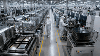
Between 2023 and 2026 the semiconductor industry witnessed a structural shift: a growing fraction of global DRAM wafer-equivalent capacity was repurposed for High-Bandwidth Memory (HBM) production. That reallocation—driven by hyperscaler commitments, higher ASP incentives, and strategic capex by major memory makers—has had a pronounced “crowding out” effect on commodity DRAM supply.