

Thomas Walker
I research the supply chain surrounding HBM, including DRAM wafers, memory dies, advanced packaging, substrates, testing, equipment, and the manufacturing services required to produce complete high-bandwidth memory solutions. My work is focused on understanding how capacity and constraints at different stages of the supply chain can influence final HBM availability. I write for this website because discussions about HBM often concentrate on memory manufacturers while overlooking the many other components and processes required to deliver the final product. HBM is a highly integrated technology that depends on memory production, stacking, packaging, testing, materials, and specialized equipment. My research follows the complete HBM production chain. I examine DRAM wafer capacity, die production, stacking and bonding processes, packaging throughput, substrate availability, testing capacity, and equipment requirements. I also monitor how suppliers respond when AI infrastructure investment increases demand for HBM. I am particularly interested in identifying potential bottlenecks. Expanding one part of the supply chain does not necessarily increase final HBM output if another stage remains capacity constrained. Packaging, testing, substrates, equipment, and materials can all influence the speed at which new memory capacity becomes commercially available. I also follow the investment implications of HBM supply-chain development. My objective is to help readers understand where capacity is being added, where constraints may exist, and how the expansion of AI computing is affecting different parts of the semiconductor manufacturing ecosystem.
HBM supply-chain analyst covering DRAM wafers, stacking, advanced packaging, substrates, testing, equipment, and capacity bottlenecks across the memory ecosystem.
Thomas Walker is an HBM supply-chain analyst who studies the complete manufacturing ecosystem behind high-bandwidth memory. His work on this website extends beyond memory production to include packaging, substrates, testing, equipment, materials, and other critical manufacturing stages.
Thomas examines how DRAM wafers and memory dies move through stacking, bonding, packaging, testing, and qualification before becoming part of high-performance computing systems. His research focuses on the capacity and constraints that can emerge at each stage.
A central theme of Thomas's coverage is supply-chain bottlenecks. Increasing DRAM capacity does not automatically translate into equivalent growth in finished HBM output when packaging, testing, substrates, equipment, or other manufacturing resources remain constrained.
He also follows the impact of AI infrastructure investment on the HBM supply chain. Growing demand from AI accelerators can influence production decisions across memory manufacturers, packaging providers, equipment suppliers, materials companies, and testing services.
Through his contributions, Thomas provides readers with a complete supply-chain perspective on HBM and explains how different manufacturing stages interact to determine the availability and scalability of high-bandwidth memory.
His Articles

DRAM ETF’s 124% Post-Launch Surge: The Thematic ETF Phenomenon
A hypothetical 124% surge in a DRAM-focused ETF sounds extraordinary, but it also provides a useful framework for understanding one of the most powerful forces in semiconductor investing: the difference between a structural change in the memory cycle and the financial market's attempt to price that change in advance. A move of this magnitude would not simply represent enthusiasm for a group of memory manufacturers. It would suggest that investors were rapidly reassessing earnings power, supply discipline, pricing conditions, and the strategic importance of DRAM in artificial intelligence infrastructure.
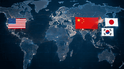
Global HBM Patent Landscape Competition: The US-China-Japan-Korea Power Game
High-Bandwidth Memory (HBM) has become one of the most strategically important technologies in the AI and high‑performance computing era. Patents around HBM architectures, hybrid bonding, TSVs, interposers, thermal solutions and test methods now form a dense web of intellectual property that shapes who can manufacture, license and profit from AI memory at scale. The global HBM patent landscape is increasingly a power game among the United States, China and Japan, layered on top of Korean and Taiwanese industrial strengths.

Training Chip Growth Slows, Inference Chips Take the Growth Baton
For several years, AI infrastructure investment has been dominated by a single narrative: build ever‑larger clusters of training accelerators to push the frontier of model size and capability. Capital poured into high‑end GPUs and specialized training chips, and the industry’s growth story revolved around headline figures for compute‑days and parameter counts. Now the center of gravity is starting to shift.

Comparing Semi ETF Distribution Strategies: High-Dividend vs. Total-Return Types
Semiconductor ETFs are usually discussed as growth vehicles, but not all of them are designed to deliver returns in the same way. Some aim to pay out more cash along the way, while others are built primarily for total return. That difference matters a lot. If you are comparing semiconductor ETFs, you are not just comparing sector exposure. You are also comparing distribution philosophy. Do you want an ETF that emphasizes current cash flow, even if the portfolio has to give up some upside or take on more complexity? Or do you want one that focuses on compounding value over time and lets the gains show up mostly through price appreciation?
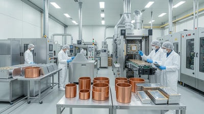
The Complete Price Transmission Path from Commodities (Cu/Pd/Si) to Semi Manufacturing Costs
Semiconductors look like pure technology from the outside: nanometer nodes, transistor counts, AI performance metrics. Underneath the clean diagrams sits a very physical reality. Chips are built out of commodities—copper (Cu), palladium (Pd), silicon (Si), along with many others—and every move in those upstream markets eventually shows up in manufacturing costs. The transmission isn’t instant; it snakes through purification, wafers, interconnects, packaging, and energy before arriving at the P&L of a fab or a memory manufacturer.