

Kevin Foster
I specialize in high-bandwidth memory and the technologies supporting modern AI computing. My research covers HBM generations, DRAM architecture, memory stacking, TSV technology, interconnects, advanced packaging, bandwidth, capacity, and the relationship between memory architecture and accelerator performance. I am particularly interested in how HBM has evolved from a specialized memory technology into a critical component of large-scale AI computing systems. I write for this website because the importance of HBM is often reduced to a discussion of memory capacity or bandwidth. In reality, HBM involves a combination of DRAM technology, vertical stacking, packaging, thermal management, interconnect design, testing, and system integration. Understanding these relationships is essential for evaluating both the technical development and commercial significance of HBM. My research follows the evolution of HBM generations and examines how improvements in density, bandwidth, stack height, power efficiency, and interface design affect AI accelerators. I also study how HBM interacts with advanced packaging technologies and how packaging limitations can influence overall system performance. Another part of my work focuses on the relationship between HBM technology and AI accelerator architecture. As AI models become larger and computing workloads become more memory-intensive, the ability to move data efficiently between processors and memory has become increasingly important. I examine how these requirements influence memory design and semiconductor manufacturing. I also follow HBM-related industry investment and supply-chain developments. Through my work, I aim to provide readers with a technically grounded understanding of HBM and explain why memory architecture, packaging, manufacturing, and AI computing demand are becoming increasingly interconnected.
HBM technology analyst specializing in high-bandwidth memory architecture, DRAM stacking, TSVs, bandwidth, density, advanced packaging, and AI accelerator integration.
Kevin Foster is an HBM technology analyst who specializes in the memory architecture supporting modern AI computing. His work on this website focuses on high-bandwidth memory, DRAM stacking, advanced interconnects, packaging, and the evolution of HBM technology.
Kevin examines the technical foundations of HBM, including memory density, bandwidth, stack structures, TSV technology, interface design, power efficiency, and thermal requirements. His research explains how these individual technologies combine to determine the capabilities of modern high-performance memory systems.
His coverage also explores the relationship between HBM and AI accelerators. As AI workloads require increasingly large amounts of data to move between processors and memory, HBM has become an important component of accelerator architecture. Kevin examines how memory requirements influence processor design and advanced packaging.
Another important area of his research is the evolution of HBM generations. He follows improvements in bandwidth, capacity, density, power efficiency, stack height, and interface technologies while examining the manufacturing and system-level challenges associated with each generation.
Through his contributions, Kevin provides readers with detailed technical insight into HBM and explains why high-bandwidth memory has become a strategically important technology within the AI semiconductor ecosystem.
His Articles

Semi ETF Options Hedging: The Put Protection Cost-Benefit
Semiconductor ETFs offer investors an efficient way to participate in the long-term growth of chip manufacturing, artificial intelligence infrastructure, memory, advanced packaging, and data-center investment. The same concentration of opportunity, however, can create significant downside risk. Semiconductor stocks can move sharply when earnings expectations change, memory prices turn, capital expenditure forecasts weaken, or technology valuations reset. For investors who want to maintain a long position while reducing the impact of a sudden decline, put options can provide a form of portfolio protection.

Analyzing the Distortion Effect of Government Subsidies on Semi FCF
Government subsidies have become a central feature of the modern semiconductor landscape. From grants and tax credits to low‑cost loans and direct equity participation, public programs now influence where fabs are built, how capacity is expanded, and which companies lead in critical technologies. On the surface, these subsidies often look like free or cheap money that improves investment economics.

A Complete Practical Guide to Building a Custom "HBM+CoWoS" Index Portfolio
High-bandwidth memory (HBM) and computing power on silicon (CoPoS) have moved from niche technical terms to the center of the AI hardware story. HBM solves the bandwidth bottleneck between compute and data; CoPoS captures the performance and efficiency of GPUs, accelerators, and custom AI chips on the silicon itself. Together, they define a large part of the infrastructure that makes modern AI training and inference possible. If you want a focused, investable representation of this hardware stack, a custom "HBM+CoPoS" index portfolio is one of the most direct ways to build it.

Long Volatility via Semi ETFs – VIX Correlation Analysis and Hedging Strategies
Semiconductor ETFs and volatility are natural neighbors, even if they do not always look that way on the surface. Semis are among the most momentum-sensitive and narrative-driven parts of the market, which means they can move sharply when risk appetite shifts. That makes them a useful place to think about long volatility. If you want to hedge a semiconductor-heavy portfolio, or simply understand when semi ETFs become a stress signal for the broader market, the relationship between semis and the VIX is worth studying closely.
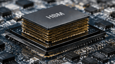
HBM’s Share of Global DRAM Capacity Exceeds 20% for the First Time in 2026
In 2026 the semiconductor industry recorded a milestone: high-bandwidth memory (HBM) has crossed the 20% threshold of global DRAM wafer-equivalent capacity for the first time. This is not merely a metric—it's a structural signal. It reflects changing customer priorities, deliberate capital allocation decisions by leading memory makers, and maturation of advanced packaging ecosystems that finally translate wafer output into finished, high-value modules at scale.