

Ethan Brooks
I research investment products focused on AI computing and the semiconductor infrastructure that supports large-scale artificial intelligence workloads. My work covers GPU and accelerator exposure, AI networking, advanced packaging, memory, and the companies supplying critical components to AI data centers. I write for this website because AI infrastructure has created a semiconductor investment theme that extends well beyond traditional chip designers. Modern AI systems require processors, high-bandwidth memory, networking, advanced packaging, storage, power infrastructure, and specialized manufacturing capacity. My research examines the holdings and construction of AI-focused ETFs and related thematic products. I study how funds divide exposure between compute, memory, networking, equipment, and other parts of the AI semiconductor ecosystem. I also follow changes in AI infrastructure spending and examine how new technology trends affect the composition of thematic funds. Through my articles, I aim to explain the structure of AI computing ETFs and how different products capture the semiconductor companies participating in the expansion of AI infrastructure.
AI computing ETF analyst covering GPUs, accelerators, networking, advanced packaging, memory, AI infrastructure, and thematic portfolio construction.
Ethan Brooks is an AI computing ETF researcher focused on investment products linked to artificial intelligence infrastructure and semiconductor technologies. His coverage includes accelerators, GPUs, networking, memory, advanced packaging, and related infrastructure.
Ethan examines how AI-focused ETFs distribute exposure across the semiconductor ecosystem. He studies the balance between compute, memory, networking, equipment, and other technologies required by large-scale AI systems.
He also follows changes in AI infrastructure investment and technology adoption. New accelerator architectures, increasing memory requirements, networking upgrades, and advanced packaging can all influence the composition of AI-themed investment products.
Through his articles, Ethan explains how AI computing ETFs are constructed and how different portfolio approaches capture the companies participating in the expansion of AI semiconductor infrastructure.
His Articles
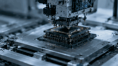
TSV Technology Iteration in HBM – New Requirements for Equipment Suppliers
Through successive HBM generations the through-silicon via (TSV) has evolved from a tactical enabling feature into a strategic differentiator. As HBM moves from HBM2E and HBM3 to HBM3e and HBM4, TSVs must support finer pitches, lower parasitics, higher thermal conduction needs, and coexistence with hybrid-bond planes. These requirements cascade into new expectations for equipment suppliers across lithography, etch, deposition, CMP, inspection, and metrology.

Quarterly Changes in Global Systemically Important Banks’ Credit Policies for Semis
Semiconductors have moved from a niche industry to the backbone of the global economy. Chips power everything from smartphones and cars to data centers and industrial robots. Behind that impressive hardware, however, sits a quieter but equally important structure: the flow of credit that finances fabs, equipment, inventory, and research. At the center of this structure are Global Systemically Important Banks (G-SIBs), whose quarterly changes in credit policies can subtly, and sometimes not so subtly, reshape the semiconductor landscape.

Long-Term Replacement Threat of Quantum Computing to AI Chips: Timing and Path
Every major technology wave eventually faces the question of succession: what comes after it, and when? AI chips—GPUs, TPUs, custom accelerators—have defined the current era of machine intelligence by enabling massive parallel computation on classical hardware. Quantum computing, with its radically different model of information processing, is often cast as a long‑term replacement threat to these AI chips. The reality is more nuanced.

A Holdings Penetration Analysis of AI Compute ETFs – How Much is Memory Exposure Underestimated?
Most AI investors can recite the usual suspects in their sleep: Nvidia, AMD, Microsoft, Alphabet, maybe a sprinkling of cloud platforms and chip designers. Ask the same investors how much memory exposure—DRAM, HBM, NAND, and storage infrastructure—they actually hold through their AI compute ETFs, and the answers get fuzzier. Yet in 2026, memory has increasingly been labeled the “biggest bottleneck” in AI, and dedicated memory ETFs have quietly exploded in assets and performance.

The Cost-Benefit of GPU Cluster Migration from InfiniBand to Ethernet (RoCE)
As AI training clusters scale from dozens to thousands of GPUs, the interconnect fabric becomes one of the largest and most strategic line items in the infrastructure budget. For years, InfiniBand has been the de facto choice for high‑performance GPU clusters, particularly in large‑scale deep learning and HPC environments. At the same time, Ethernet with RDMA over Converged Ethernet (RoCE) has quietly matured, closing much of the performance gap while retaining the economic and operational advantages of mainstream Ethernet ecosystems.
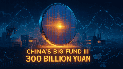
Big Fund III’s 300B Yuan Allocation: Equipment, Materials, and HBM Breakdown
China’s third national semiconductor investment vehicle—commonly referred to as “Big Fund III”—marks a new phase in the country’s effort to build a more self‑sufficient and globally competitive chip ecosystem. With a planned war chest on the order of 300 billion yuan, the fund is widely expected to pivot from simply backing wafer capacity toward deeper, more targeted investments in equipment, materials, and memory technologies such as high‑bandwidth memory (HBM).