

Daniel Carter
I specialize in 3D semiconductor integration and the technologies that allow multiple layers of active and passive components to be combined within increasingly compact systems. My research covers 3D IC architecture, vertical interconnects, TSVs, wafer bonding, thermal management, and manufacturing challenges. I write for this website because three-dimensional integration is becoming increasingly relevant as conventional scaling becomes more difficult and system designers seek additional ways to improve performance and density. My research examines 3D stacking approaches across logic, memory, and advanced packaging. I follow developments in vertical integration, die stacking, thermal management, interconnect density, and manufacturing yields. I also study the relationship between 3D integration and AI computing. High-performance processors and memory systems increasingly require greater bandwidth and shorter interconnect distances, creating new opportunities for vertically integrated architectures. My goal is to provide readers with a clear understanding of the technology and economics behind 3D ICs and explain how vertical integration may influence future semiconductor architectures.
3D IC researcher covering vertical integration, TSVs, die stacking, wafer bonding, thermal management, interconnect density, and advanced semiconductor architectures.
Daniel Carter is an advanced packaging researcher focused on 3D IC technologies and vertical semiconductor integration. His coverage includes die stacking, TSVs, wafer bonding, vertical interconnects, and thermal management.
Daniel examines how three-dimensional integration can increase system density and reduce interconnect distances. His research spans memory, logic, and high-performance computing applications where conventional two-dimensional scaling may face increasing limitations.
Thermal management and manufacturing yield are important themes in his work. As more components are integrated vertically, heat dissipation, alignment, bonding quality, and process reliability become critical engineering considerations.
Daniel also studies the relationship between 3D integration and AI computing. Through his articles, he explains how vertical architectures may support higher bandwidth, greater integration density, and new approaches to future semiconductor system design.
His Articles
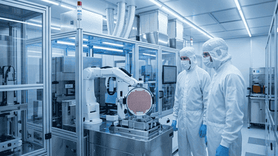
Memory HHI Concentration: The Pricing Power Shift
Memory markets have always been cyclical, but the structure of the cycle can change dramatically when industry concentration rises. For investors studying AI storage and computing power themed ETFs and index derivatives, this structural shift matters because memory pricing is not determined solely by unit demand. The number of meaningful suppliers, the distribution of production capacity, technology leadership, inventory discipline, and the intensity of AI-related demand can all influence how quickly supply responds to changes in consumption.
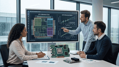
Custom Silicon for Inference: Why Hyperscalers Are Designing Their Own LPUs
The economics of AI change when a model moves from development into daily use. Training attracts attention because it requires spectacular computing resources. Inference creates the recurring bill: every search, generated answer, recommendation, and coding suggestion consumes computing capacity.

Practical Breakthroughs of Domestic EDA Tools in AI Chip Design (Huada/Prime)
As AI chips surge to the forefront of national technology strategies, attention has increasingly turned from fabs and packaging to a crucial but less visible layer: electronic design automation (EDA). For many years, domestic EDA tools lagged behind international leaders, limiting how far local firms could push advanced AI chip design without external dependencies.

The CoWoS Capacity Allocation Game: Who Gets a Bigger Slice from TSMC?
In the mid‑2020s, one of the most strategic bottlenecks in the global AI hardware ecosystem is not just advanced logic wafer capacity, but advanced packaging capacity—and in particular, TSMC’s CoWoS (Chip‑on‑Wafer‑on‑Substrate) lines. As AI accelerators, high‑bandwidth memory (HBM) stacks, and multi‑die systems proliferate, securing a larger slice of CoWoS capacity has become a competitive game played by the world’s largest chip and cloud companies.

Sovereign Wealth Funds’ Rising Allocation Ratios to Strategic Semi Assets
Sovereign wealth funds (SWFs) live at the intersection of politics, macroeconomics, and long‑term investing. They exist to turn national surpluses—often sourced from commodities, exports, or foreign exchange reserves—into enduring wealth. In the 2020s, one asset class has moved from “interesting” to “strategic” in that mission: semiconductors. Chips are now seen as part of national security and industrial policy as much as financial opportunity. That shift has forced SWFs to think hard about how much risk they are willing to allocate to semi assets, and how that allocation fits into a world of changing interest rates, exchange rates, credit cycles, and commodity prices.