

Charles Foster
My research focuses on CMP and semiconductor polishing materials used to achieve the surface quality required for advanced wafer fabrication. I study slurry technologies, polishing processes, material selectivity, wafer planarization, and the growing importance of surface control in modern semiconductor manufacturing. I write for this website because CMP is a critical manufacturing step that is often less visible than lithography or etching. However, increasingly complex device structures require extremely precise surface control between process layers, making polishing materials an important part of the semiconductor manufacturing ecosystem. My work follows CMP slurry demand, polishing requirements, process complexity, material consumption, and supplier developments. I also examine how changes in logic, memory, and advanced packaging processes can influence demand for polishing materials. Another part of my research is the connection between process complexity and materials intensity. More manufacturing steps and increasingly demanding surface specifications can increase material consumption and create opportunities for specialized suppliers. Through my articles, I aim to explain CMP technology in practical terms and show how polishing materials contribute to semiconductor yield, manufacturing efficiency, and advanced process development.
Semiconductor materials researcher focused on CMP slurries, wafer planarization, polishing processes, surface control, and materials demand in advanced fabrication.
Charles Foster is a semiconductor materials researcher specializing in chemical mechanical planarization, commonly known as CMP. His work focuses on polishing materials, slurry technologies, surface control, and wafer planarization.
Charles examines how CMP requirements evolve as semiconductor structures become more complex. Precise surface control is essential between manufacturing layers, making polishing performance increasingly important to advanced semiconductor production.
His research covers slurry demand, material selectivity, polishing processes, wafer surface quality, and process efficiency across logic, memory, and advanced packaging applications.
Charles also studies the relationship between manufacturing complexity and materials consumption. Increasing process steps and tighter surface specifications can change demand for specialized CMP materials and influence the competitive landscape among suppliers.
Through his articles, Charles provides readers with a practical perspective on CMP and explains how polishing materials contribute to semiconductor yield, process control, and advanced manufacturing.
His Articles

Yongding’s $1.13B Laser Chip Orders: The Hidden Supply Chain Behind AI Infrastructure
The most important correction comes before the investment thesis: Yongding’s disclosed laser-chip orders total approximately RMB 1.133 billion, not US$1.13 billion. The July 29, 2026 announcement identified a RMB 542 million order and a US$87 million order, translated at approximately RMB 591 million. Both amounts included tax. The combined value was roughly US$167 million at the exchange rate implied by the announcement.

VIX Spikes and Semi Stock Defense: The Portfolio Strategy
Semiconductor stocks have become one of the most important expressions of the global technology cycle, but their strong growth characteristics also make them particularly sensitive to changes in financial-market conditions. When volatility suddenly rises, semiconductor equities can experience sharp price movements even when the underlying business outlook has not changed materially.

DRAM ETF’s $10B Milestone: The Fastest Thematic Launch Ever
It took 18 months. That's all it took for the first pure-play DRAM ETF to cross $10 billion in assets under management. Launched in early 2025 with modest fanfare—a niche product for a niche audience—the DRAM ETF (ticker: DRAM, hypothetical for this discussion) has become the fastest-growing semiconductor-themed ETF in history. Faster than the AI ETF boom of 2023. Faster than the EV ETF surge of 2021. Faster than the cannabis ETF frenzy of 2018.

Global AI Accelerator Market Breaks $250B in 2026: A Supply Chain Teardown
By 2026, AI accelerators have moved from niche hardware to the beating heart of modern compute, powering everything from frontier model training to real‑time inference across clouds, enterprises, and edge devices. Crossing the $250 billion mark in annual market value is not just a milestone; it is a reflection of a vast, intricate supply chain that stretches from design labs and fabs to packaging houses, board makers, system integrators, and the services that wrap around them. Understanding how this value is created and captured requires a teardown of the AI accelerator supply chain, layer by layer.
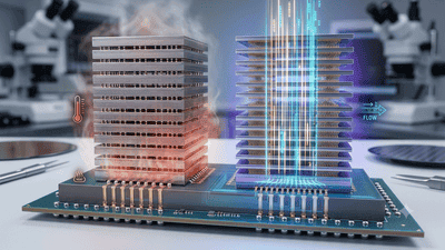
The Layer Stack and Thermal Bottleneck Breakthroughs in the HBM3E-to-HBM4 Upgrade
Upgrading from HBM3E to HBM4 represents one of the most technically challenging—and most consequential—evolutions in modern memory engineering. HBM4 promises higher signaling rates, greater per-die capacity, and improved energy efficiency per bit, but achieving those gains requires rethinking the layer stack, interconnect strategies, and thermal management at the package level.

Path Decay and Optimal Holding Window Analysis for 3x Leveraged Semi ETFs
Triple-leveraged semiconductor ETFs are exciting for the same reason they are dangerous: they magnify movement. When semiconductors are trending strongly, a 3x product can feel like the most efficient way to express a bullish view. When the sector turns choppy, however, the same product can bleed value quickly even if the underlying index is not collapsing. That is the core problem of path decay. It is not just about whether the market goes up or down. It is about the route the market takes to get there.