

Alexander Reed
I research the rapidly evolving AI accelerator market, including GPU platforms, custom silicon, inference processors, networking chips, and emerging accelerator architectures. My work combines semiconductor architecture with manufacturing, packaging, software compatibility, and data-center deployment. I am interested in how the entire computing platform influences the commercial value of an AI processor. I joined this publication to provide readers with a broader view of AI semiconductor competition. Product specifications are important, but they do not fully explain the position of an accelerator in the market. Software ecosystems, developer tools, memory systems, networking, power efficiency, manufacturing availability, and system integration can be equally important. My research compares general-purpose GPUs with custom ASICs and other specialized processors. I examine how different designs address training and inference workloads, how customers balance flexibility and efficiency, and why certain applications may favor customized silicon. I also follow the development of inference hardware for cloud, enterprise, automotive, and edge applications. I pay close attention to the relationship between accelerator design and advanced packaging. High-performance AI processors increasingly require high-bandwidth memory, complex interconnects, and advanced thermal solutions. These requirements influence manufacturing capacity and create opportunities across several semiconductor supply-chain segments. I also follow AI infrastructure investment and its implications for semiconductor companies. My goal is to explain how processor roadmaps, customer requirements, manufacturing constraints, and system-level economics interact. Through this website, I aim to provide balanced and practical research for readers following the AI chip industry.
AI hardware researcher covering GPU platforms, custom ASICs, inference processors, networking silicon, software ecosystems, and data-center system integration.
Alexander Reed is an AI hardware researcher who studies the rapidly changing market for GPUs, custom ASICs, inference processors, and networking silicon. His coverage on this website examines AI semiconductor products from both architectural and system-level perspectives.
Alexander focuses on the factors that determine the practical value of an AI accelerator. In addition to processor performance, his research considers software compatibility, developer tools, memory systems, networking, power efficiency, manufacturing availability, and data-center integration.
His articles compare general-purpose GPUs with customized and specialized processors. He examines how different architectures address AI training, inference, cloud computing, enterprise workloads, and edge applications, while also considering the trade-offs between flexibility, efficiency, and development cost.
Alexander also follows the packaging and manufacturing requirements of advanced AI processors. High-bandwidth memory, complex interconnects, thermal management, and advanced process technologies are becoming increasingly important to accelerator design and production.
Through his work, Alexander helps readers understand the competitive and technical forces shaping the AI semiconductor ecosystem, from processor architecture and software support to manufacturing capacity and data-center deployment.
His Articles

Inference Era Pricing: Why LPU Architecture Targets the Token Generation Bottleneck
The price of an AI response depends on more than how much arithmetic a chip can perform. It depends on how quickly the system accesses data, how efficiently it schedules requests, and whether the resulting answer arrives within the application’s time limit.

China’s TPU Breakthrough: How Zhonghao Xinying Filled the Pure TPU Architecture Gap
China’s AI chip industry is often discussed through GPUs and neural-processing units. Zhonghao Xinying offers another route: a processor designed around tensor computation, supported by its own instruction set and computing platform.

Korea Memory Duo in MSCI Korea: The Dominance Trend
The structure of the Korean equity market has created an unusual bridge between country-level index investing and the global AI infrastructure cycle. Samsung Electronics and SK hynix are not merely two large semiconductor companies operating in the same region. Together, they provide investors with highly concentrated exposure to memory, high-bandwidth memory, AI servers, advanced semiconductor manufacturing, and the broader technology investment cycle.
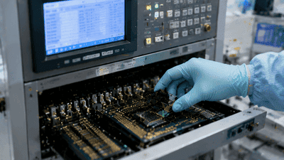
Incremental Demand for HBM Test and Burn-in Equipment – A Quantified Forecast
As High-Bandwidth Memory (HBM) moves from niche to mainstream across AI, HPC, and advanced graphics, test and burn-in equipment emerges as a critical bottleneck. HBM modules require more extensive, higher-fidelity testing than commodity DRAM: multi-die functional tests, high-speed channel validation, thermal stress profiles, and system-level burn-in under representative accelerator loads.
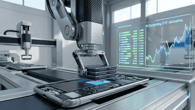
A High-Frequency Leading Indicator Model Linking Memory Indices and PC/Smartphone Shipments
In technology markets, most of the attention goes to the shiny devices we can see and touch: PCs, laptops, smartphones, tablets. Yet the real heartbeat of those markets often lies in something far more invisible — memory. DRAM, NAND, and related storage components set the pace for production, shape margins, and quietly telegraph where demand is headed before shipment reports or earnings calls ever arrive. If you want to build an ETF or index derivative around AI storage and computing power, learning to read those memory signals is not just helpful; it is foundational.
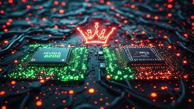
Nvidia B200 vs. AMD MI400: The 2026 AI Chip Crown Battle
By 2026, the race to power large‑scale artificial intelligence has crystallized into a few headline contests, and one of the most closely watched is the emerging battle between Nvidia’s B200 platform and AMD’s MI400 series. Both families target the same high‑stakes arena: training and inference for frontier‑scale models, hyperscale data centers, and enterprise AI deployments that push compute, memory, and networking to their limits.

Price Divergence Trading Strategies Between NAND Flash and DRAM ETFs
NAND flash and DRAM sit at the core of AI storage and computing power. Both are memory, but they are not the same business. DRAM is main memory—fast, volatile, and central to high‑bandwidth workloads like AI training and inference. NAND is non‑volatile storage—slower than DRAM, but crucial to persistent data and large‑scale object storage. The cycles that drive their pricing and margins overlap, yet they often diverge. That divergence is where trading strategies between NAND and DRAM ETFs become interesting.

Concentration Risk: What Does It Mean When Top 3 Holdings Exceed 45% in Semi ETFs?
When the top three holdings in a semiconductor ETF exceed 45% of the portfolio, the fund stops being a simple basket and starts behaving more like a bet on a small cluster of companies. That does not automatically make it bad, but it does change what you are really buying. In semiconductors, where a few names can dominate industry sentiment and earnings momentum, concentration can be a feature. It can also be a trap.

Rolling Alpha Comparison of the Pure-Play Memory ETF (MEM) vs. Broad Semi ETFs
A pure play memory ETF like MEM sits right at the heart of AI storage demand. It focuses on DRAM, NAND, and HBM names that supply the bandwidth and capacity modern AI workloads need. Broad semiconductor ETFs, by contrast, spread exposure across logic, compute, equipment, foundry, analog, and memory. When you compare their performance over time, you are really asking a deeper question: does concentrating on memory produce persistent alpha, or does it deliver bursts of outperformance and underperformance that net out over cycles?